Research Equipment
Analysis Tools
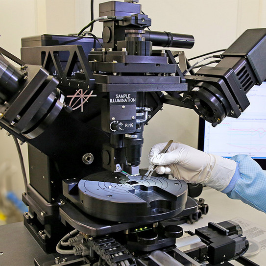
Description:
Ellipsometer
Features:
Layer thickness measurement and parameter extraction
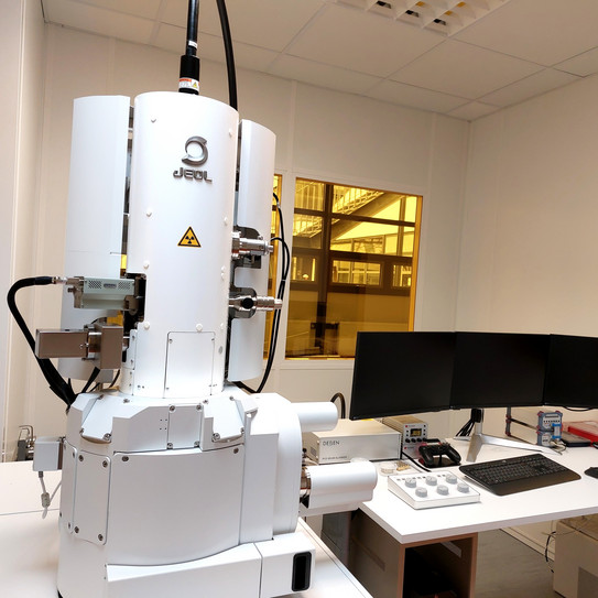
Description:
Scanning electron microscope (SEM)
Features :
Deben Beam Blanker, Kleindiek Nanotechnik Stage, Xenos Pattern Generator, Resolution down to 0,7nm
In Cooperation with Terahertz Spectroscopy Group (AG Lange)
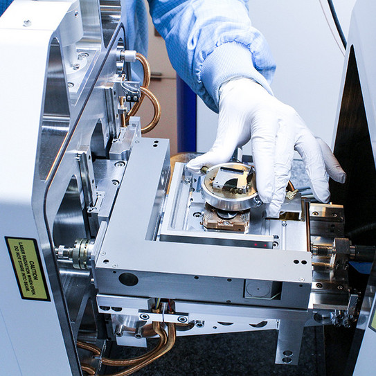
Description:
Scanning electron microscope (SEM)
Features :
Resolution up to 10nm, InLens and SE-detector
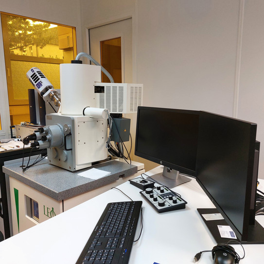
Description:
Scanning electron microscope (SEM)
with PointElectronic Elektronik Upgrade and Raith ELPHY Quantum
Features:
Up to 10 nm resolution including a 4k imaging system, topology display, InLens-, SE- and BSE-detector
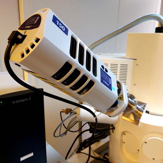
Description:
Energy-dispersive X-ray spectroscopy (EDX) system
Features:
Low-KV EDX system, ≤127eV @ MnKα, detection of elements starting from Beryllium at a minimum atomic number of Z=4 and higher
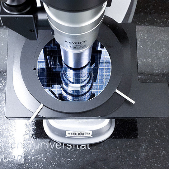
Description:
Digital optical microscope
Features:
Up to 5000x magnification
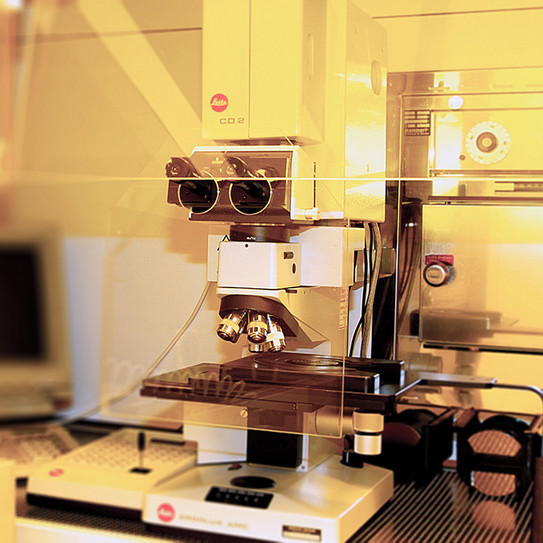
Description:
Structure Width Measuring System
Features:
Laser Autofocus
Description:
Compound microscope
Features:
Optical UIS2/UIS (Universal Infinity System)-system
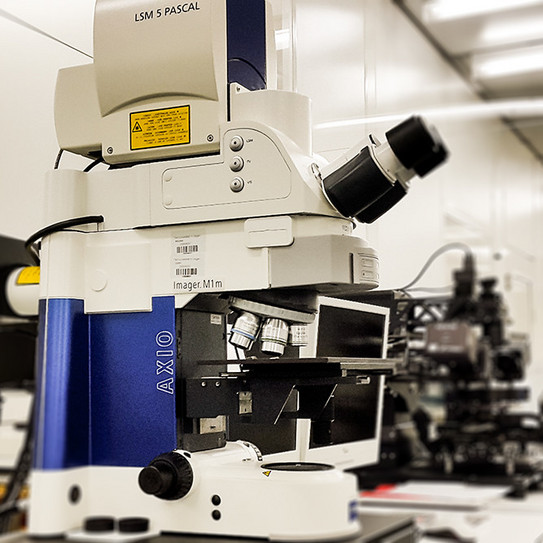
Decription:
Confocal laser microscope
Description:
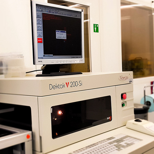
Profilometer
Features:
Surface profilometry up to 262 µm
Description:
Raman-Spectroscopy and Atomic Force Microscopy
Features:
2 Laser Sources (355 nm and 488 nm), Linkam-Stage (196 °C to +600 °C in variable atmosphere) with micro manipulators and probe needles, Atomic force microscopy (AFM, CAFM)

Measurement Instruments
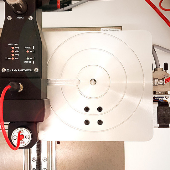
Description:
Four-point measurement system
Features:
Sheet resistance measurement on specimen pieces and wafers
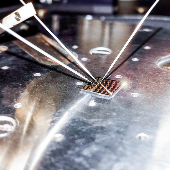
Description:
Analytical Wafer Prober
Features:
Light protected measurement station including vacuum chuck and 8 measuring needle tips
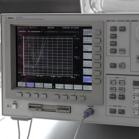
Description:
Parameter analyser
Features:
Precision Semiconductor Parameter Analyzer
Description:
Wafer prober
Features:
Full automatic wafer prober for statistic measurement of device parameters
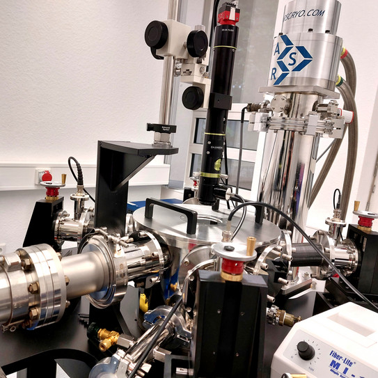
Description:
Cryogenic Probe Station
Features:
Closed Cycle, Helium Compressor, Beryllium DC probe Tips
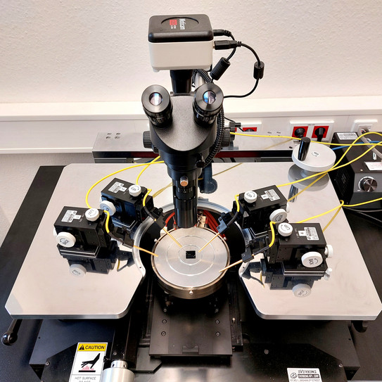
Description:
RF Wafer Prober
Features:
RF Measurements up to 40GHz, Temperature Range up to 200°C, metric screws only
Description:
Impedance Analyzer
Features:
Impedance analyzer and precision LCR meter, 1 mHz to 5 MHz, 1 mΩ to 1 TΩ
Features:
DC - 600 MHz Lock-in Amplifier, 14 bits, 1.8 GSa/s, ±150 mV, ±1.5 V (high-impedance load), -12.5 dBm, 7.5 dBm (50 Ω load), Spectrum Analyzer
Features:
Source Meter Unit (Range 1 aA - 100 mA, 1 µV - 200 V)
Features:
Source Meter Unit (0.1 fA - 10 A, 5 µV - 200 V)
Features:
Digital Nano-Voltmeter (< 1 µV - 100 V)
Features:
4x 1 GHz (5 GSPS) Oscilloscope
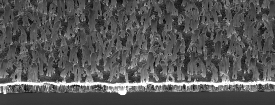
Etching Technology
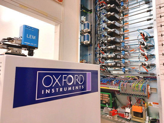
Description:
Inductive Coupled Plasma (ICP), Reactive Ion Etching (RIE)
Features:
12 different Gaslines, Fluorine- Chlorine and Bromine-Processes, End-Point Detection
Description:
Inductive Coupled Plasma (ICP), Reactive Ion Etching (RIE)
Features:
Fluorine- and Chlorine-Processes
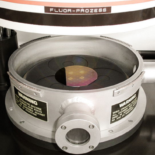
Description:
Reactive Ion Etching (RIE)
Features:
Chlorine chamber: SF6, Cl2, CHF4, SiCl4, N2; Fluorine chamber: SF6, O2, Ar, CHF3, N2
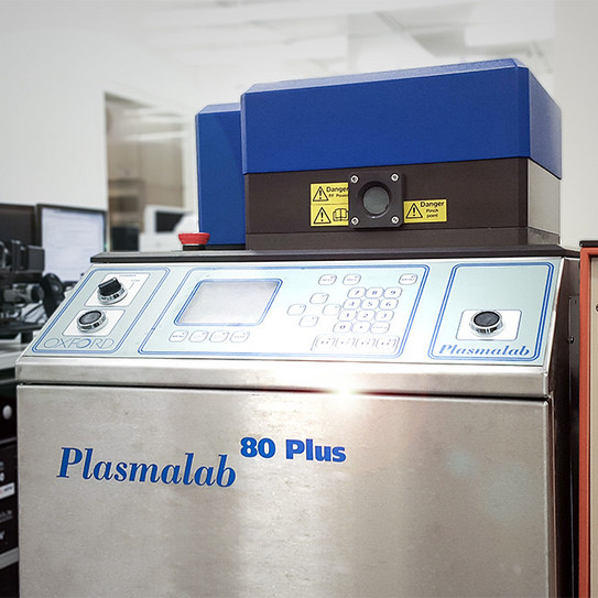
Description:
Reactive Ion Etching (RIE)
Features:
Fluorine processes: SF6, O2, Ar, CHF3, N2
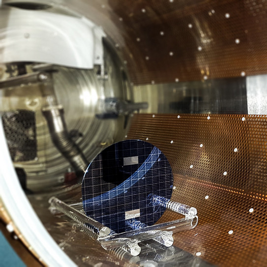
Description:
Plasma ashing
Features:
Etching via oxygen plasma, max. 8-inch wafer
Implantation and Doping Technology
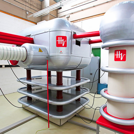
Description:
Ion Implanter
Features:
Doping reaching a max. dose of 10e16 cm-2 and a max. ion energy of 350 keV.
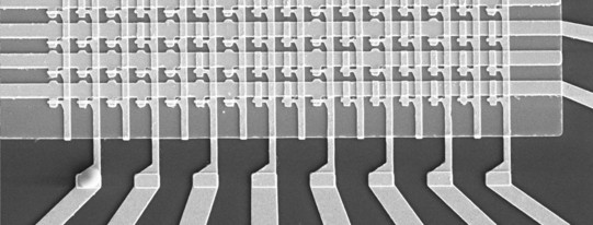
Lithography

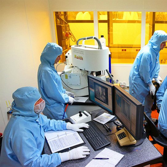
Description:
Scanning electron microscope (SEM)
Features :
Deben Beam Blanker, Kleindiek Nanotechnik Stage, Xenos Pattern Generator, Resolution down to 0,7nm
In Cooperation with Terahertz Spectroscopy Group (AG Lange)
Description:
Electron Beam Lithography (EBL)
Features:
Patterns sizing down to 10 nm on die substrates, laser interferometer controlled stitching
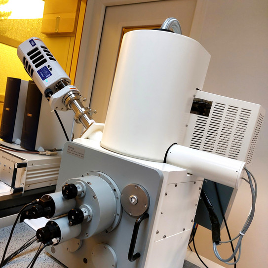
Description:
E-Beam Lithography (EBL),
includes PointElectronic Upgrade and Raith ELPHY Quantum Lithography Extension
Features:
Patterns sizing down to 10 nm on die substrates
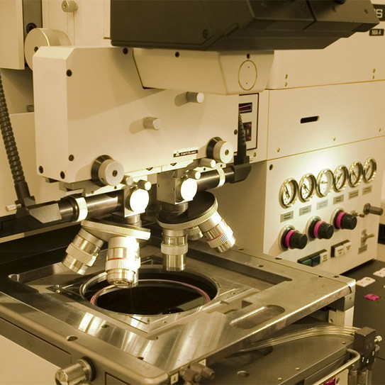
Description:
Direct exposure system
Features:
Minimum pattern resolution of 300 nm
Description:
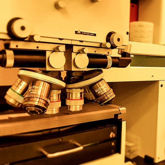
UV light exposure system, mask aligner
Features:
Structure widths down to 0,6 µm on 4 inch substrates
Description:
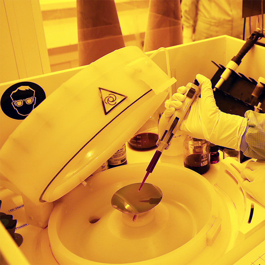
UV light exposure system, mask aligner
Features:
Structure widths down to 0,6 µm on 4 inch substrates
Description:
Spin coating system
Features:
Wafer sizes up to 200 mm, rotational speeds up to 12000 RPM
Description:
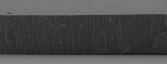
Spin Coating System
Features:
Wafer sizes up to 200 mm, rotational speeds up to 12000 RPM, used for silicones
Thin Film Deposition
Description:
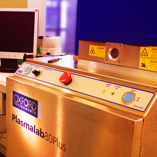
Atomic Layer Deposition
Features:
Thermal ALD up to 500°C, Glovebox, Picozone™ PZ-100 ozone generator, Precursor: TMA, TEMAHf, H2O, NH3
Description:
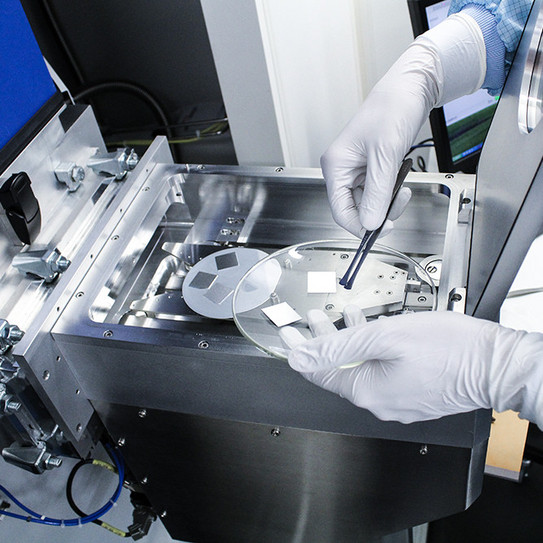
Plasma Enhanced Chemical Vapor Deposition (PECVD)
Features:
Thin film deposition by Chemical Vapor Deposition
Description:
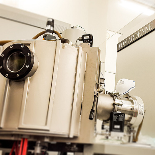
Reactive Magnetron Sputtering
Features:
Physical Thin Film Depositon (feat. Al, Ti [ TiN reactive], Ni, Si)
Description:
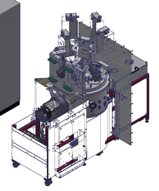
Reactive Magnetron Sputtering
Features:
Depostion of ITO, Lanthanum hexaboride, Samarium, Yttrium and Bismuth telluride
Description:
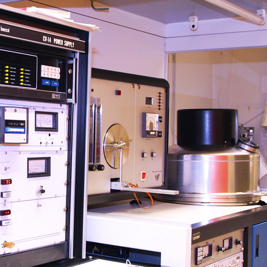
Confocal DC/RF magnetron sputtering system with plasma emission monitor (PEM)
Features:
Deposition of chromium, niobium (-oxide), and hafnium (-oxide), as well as other materials
Description:
Evaporation
Features:
Contains Al-target and Cr-target
Description:
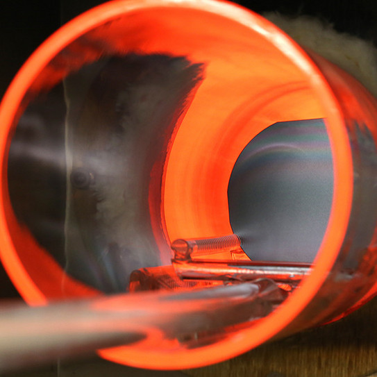
Diffusion and oxidation furnace
Features:
Oxidation (wet and dry), H2 and N2 tempering
Description:
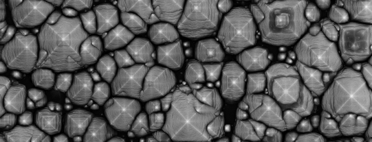
Low Pressure Chemical Vapour Deposition (LPCVD), Diffusion and oxidation furnace
Features:
LPCVD, Oxidation (wet and dry), H2 and N2 tempering, temperature range up to 1250°C
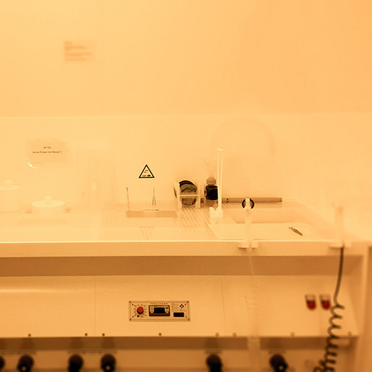
Wet Benches
Description:
Wet etching processes for SiO2, Si3N4, Al and Au
Beschreibung:
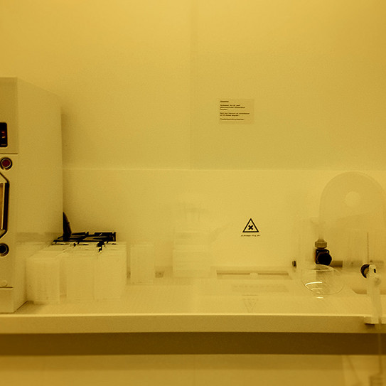
Development of various resists (AZ resists, PMMA etc.)
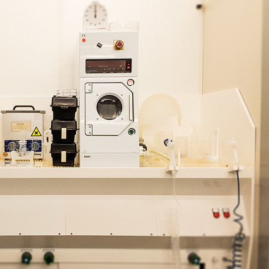
Description:
Wafer cleaning SC1, SC2
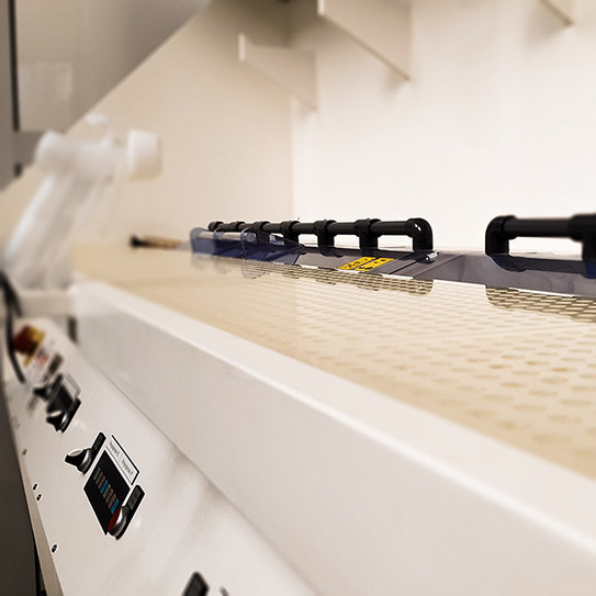
Description:
Cleaning of horizontal furnaces
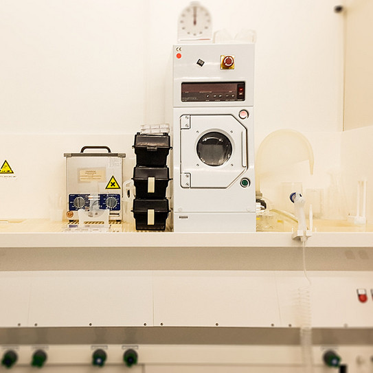
Description:
Spin Rinser
Cleanroom
Description:
Fan Filter Units
Features:
Laminar flow areas at each working station
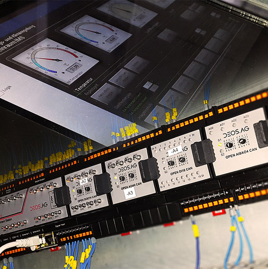
Beschreibung:
Air treatment according to ISO 14644, 21.0°C, 45%rF, 12 Pa overpressure
Features:
DEOS OPEN 500EMS, Carrier 30RA160B, 158kW cooling capacity, Vapac LE90 electrode humidifier
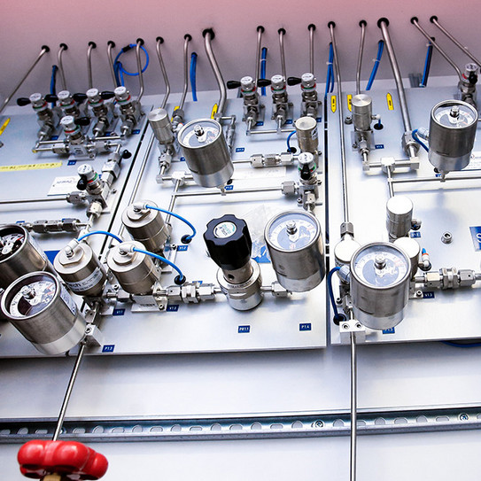
Description:
SPS supported custom design
Features:
Provides O2, N2, Ar, Cl2, SiCl4, H2, N2O, CF4, CHF3, SF6, NH3, SiH4/Ar, SiH2Cl2
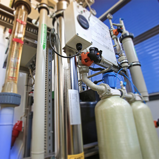
Description:
Ultrapure Water Supply (UV treated)
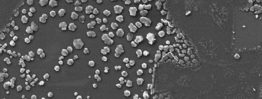
Others
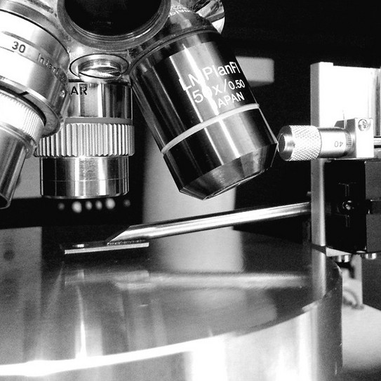
Description:
In-House development
Sample-To-Sample Transferprozesse of 2D nanomaterials
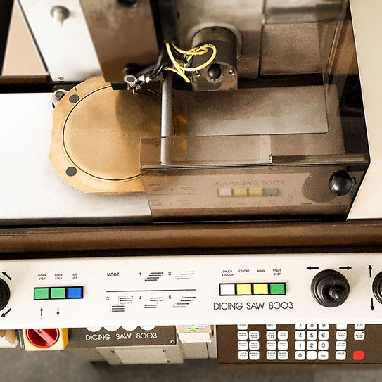
Description:
Wafer Saw
Features:
Wafer sizes ranging from 25.4 to 152.4 mm, wafer thicknesses ranging from 10 to 5000 µm, blade rotation 15000 - 45000 RPM
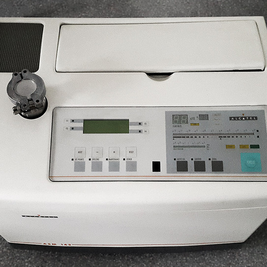
Description:
Portable Leak Detector
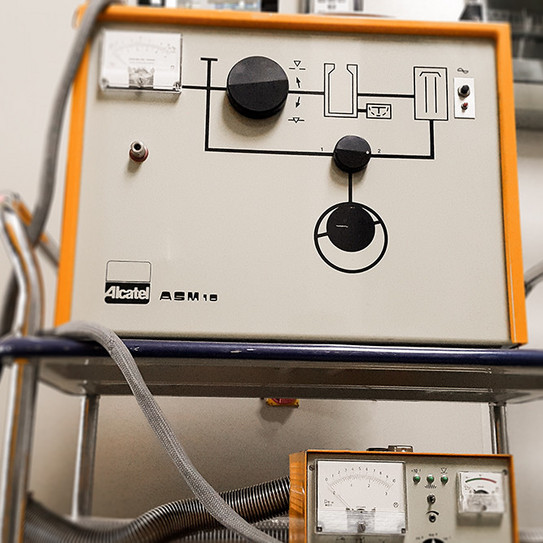
Portable Helium Leak Detector
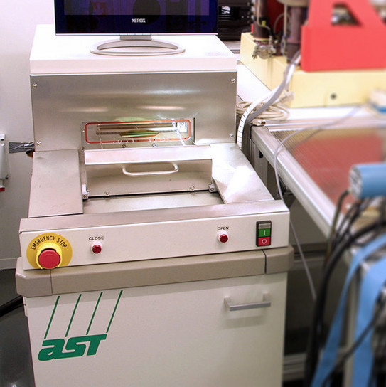
<font face="Akkurat-Bold, sans-serif">Description:</font>
Rapid Thermal Annealing up to 1200°C in Ar/H2/N2 atmosphere, substrate sizes up to 6 Inches
Description:
n/a
Description:
C4 galvanic solder deposition (bumps)
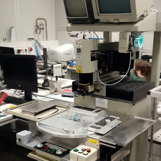
Description:
Ultrasonic Heavy Wire Bonder (400µm)

