DFG Major Research Instrumentation
Confocal DC/RF Magnetron-Sputter-System
Confocal sputtering (co-sputtering) is a physical vapor deposition (PVD) processes, which allows for deposition of functional heterostructures by means of cathode sputtering using multiple confocally arranged sputter sources. Confocal sputtering differs from classical sputtering in that several sputter sources are operated in simultaneously.
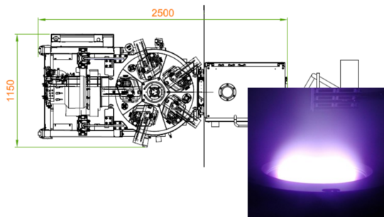
Within the scope of this proposal, the procurement of a DC/RF sputtering system with confocally arranged cathodes is requested for the implementation of innovative research projects. Research of the Chair of Micro- and Nanoelectronics is focused on novel semiconducting and functional thin-films and low-dimensional materials, which find application in novel electronic devices, information technology, sensor technology and micro- and nanosystems. The co-sputter system will be an integral part of the technology required to carry out innovative research projects ranging from fundamental to applied science.
Unlike conventional sputtering processes, co-sputtering allows not only the sequential deposition of different material layers but also a continuous change of the layer composition with high flexibility. In combination with inert gases, the use of reactive gases such as oxygen or nitrogen offers the possibility of depositing thin layers of oxides and/or nitrides. This combination of process parameters opens up completely new possibilities in the deposition of innovative and functional thin-films. Within the context of future-oriented research projects, heterostructures based on transition metal oxides with tunable stoichiometry and defect density are to be realized. Such material systems find application in the field of novel nanostructured sensors, thermo- and pyroelectrics as well as plasmonics. Furthermore, co-sputtering allows the fabrication of thin-films with complex dopant profiles and in situ controllable dopant concentration, which cannot be realized by classical doping methods. In this way, nanoionic processes can be used in highly integrated memristors for applications in the field of neuromorphics.
Within the scope of this proposal, research projects will also be carried out by other users from the departments of electrical engineering and information technology as well as physics within the TU Dortmund and in the future also within the Research Alliance Ruhr. In this way, the deposition system will be a key tool for excellent cross-faculty projects and forms the basis for further interdisciplinary synergies in the medium term.
DFG Major Research Instrumentation Art. 91b GG
- Titel: Confocal DC/RF Magnetron-Sputter-System
- Project Number: 515777855
- Project Duration: Since 2023
- Funding: 50 % DFG, 40 % State NRW, 10 % TU Dortmund University


High-Resolution Raman-Atomic-Force-Microscopy
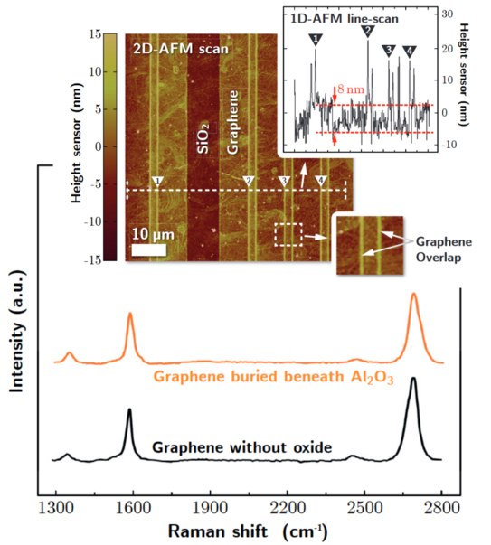
Raman spectroscopy is based on inelastic scattering of light within solids. It is a power technique to investigate the chemical composition, mechanical stress as well as crystallinity and crystal-orientation of thin-films. In this proposal we apply for funding for a combined high-resolution Raman- and Atomic-Force-Microscope.
Research of the group of Prof. Tappertzhofen (Chair for Micro- and Nanoelectronics, TU Dortmund University) is focused on fabrication and modification of semiconductor, multifunctional and novel low-dimensional materials. These materials are the building blocks for new micro- and nanoelectronic devices for application in information technology, sensor systems, photonics and micro- and nanosystems. The combined high-resolution Raman- and Atomic-Force-Microscope will be an integral part of the group’s research infrastructure. The proposed measurement system will combine the high sensitivity (stoichiometry, crystallinity and interface stress) of two-dimensional Raman spectroscopy with the ultra-high lateral resolution of Atomic-Force-Microscopy.
With its powerful analytic capabilities, the microscope system will enable to carry out challenging and original research-projects targeting fundamental and application-oriented aspects. In particular, we will use this high-resolution technique to investigate the chemical composition and crystallinity of memristively switching transition-metal-oxides for neuromorphic applications. In another project, the measurement system will be used to analyze defects and the morphology of low-dimensional materials at the same lateral position. Based on these findings novel tunnel field effect transistors will be fabricated and investigated. In combination with a dedicated sample chamber for adjusting variable temperatures and atmospheres physico-chemical phenomena of multifunctional materials will be investigated in situ. Special attention will be paid to the interplay of nanoionic redox-reactions in thin-films with the ambient gas. These materials have a high application potential for advanced nano-structured sensor technology.
The measurement system will be operated by users based in the electrical engineering and information technology, chemistry, and bio-chemical engineering departments. It will thus take a key role in original research projects across departments and will enable future interdisciplinary synergies.
DFG Major Research Instrumentation Art. 91b GG
- Titel: High-Resolution Raman-Atomic-Force-Microscopy
- Project Number: 507298853
- Project Duration: Since 2022/23
- Funding: 50 % DFG, 40 % State NRW, 10 % TU Dortmund University


Atomic Layer Deposition System
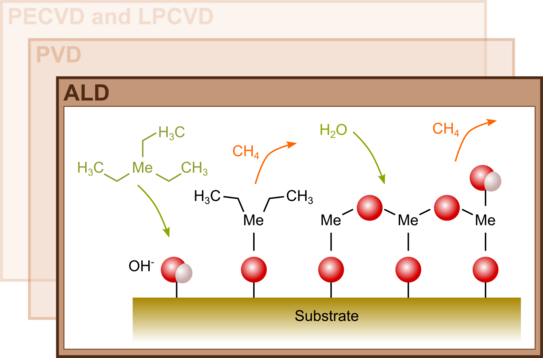
Within this project an atomic layer deposition (ALD) system will be purchased that is capable to handle substrates with a diameter of up to 200 mm. The ALD system will be used to deposit functional (e.g. multiferroic or memristive) oxides and nitrides, and catalytically active metals. These materials will be integral parts in novel electronic devices and circuits for application in information technology, photonics, micro-fluidics, and micro- and nanotechnology. ALD is the only technology that provides the specific deposition properties (including precise control of thickness and stoichiometry, conformal deposition, and low deposition temperature and energy) required to perform the planned cutting-edge research projects.
The ALD system will be used to deposit functional (e.g. multiferroic or memristive) oxides and nitrides, and catalytically active metals. These materials will be integral parts in novel electronic devices and circuits for application in information technology, photonics, micro-fluidics, and micro- and nanotechnology. ALD is the only technology that provides the specific deposition properties (including precise control of thickness and stoichiometry, conformal deposition, and low deposition temperature and energy) required to perform the planned cutting-edge research projects.
DFG Major Research Instrumentation Art. 91b GG
- Titel: Atomic Layer Deposition System
- Project Number: 471301649
- Project Duration: Since 2022
- Funding: 50 % DFG, 40 % State NRW, 10 % TU Dortmund University


